IBM debuts sub-1 nanometer chip technology (newsroom.ibm.com)
366 points by porridgeraisin a day ago
buran77 a day ago
> logic technology can extend for the first time below the 1 nm node, advancing the era of angstrom-level scaling, where dimensions approach the size of individual atoms. While transistor nodes now refer to a generation of manufacturing technology versus an exact physical dimension, IBM’s 0.7 nm technology—also referred to as 7 angstroms—demonstrates how continued scaling remains possible.
Continuing the well established trend of making bold claims about physical dimensions that have nothing to do with any of the structures in the chip, and the name scales better than the tech.
What they actually deliver is a "nanostack architecture" built with ~5nm features that according to them is comparable to a hypothetical real sub-1nm chip.
It's an impressive achievement nonetheless but it looks like the industry has a few too many marketers.
adrian_b a day ago
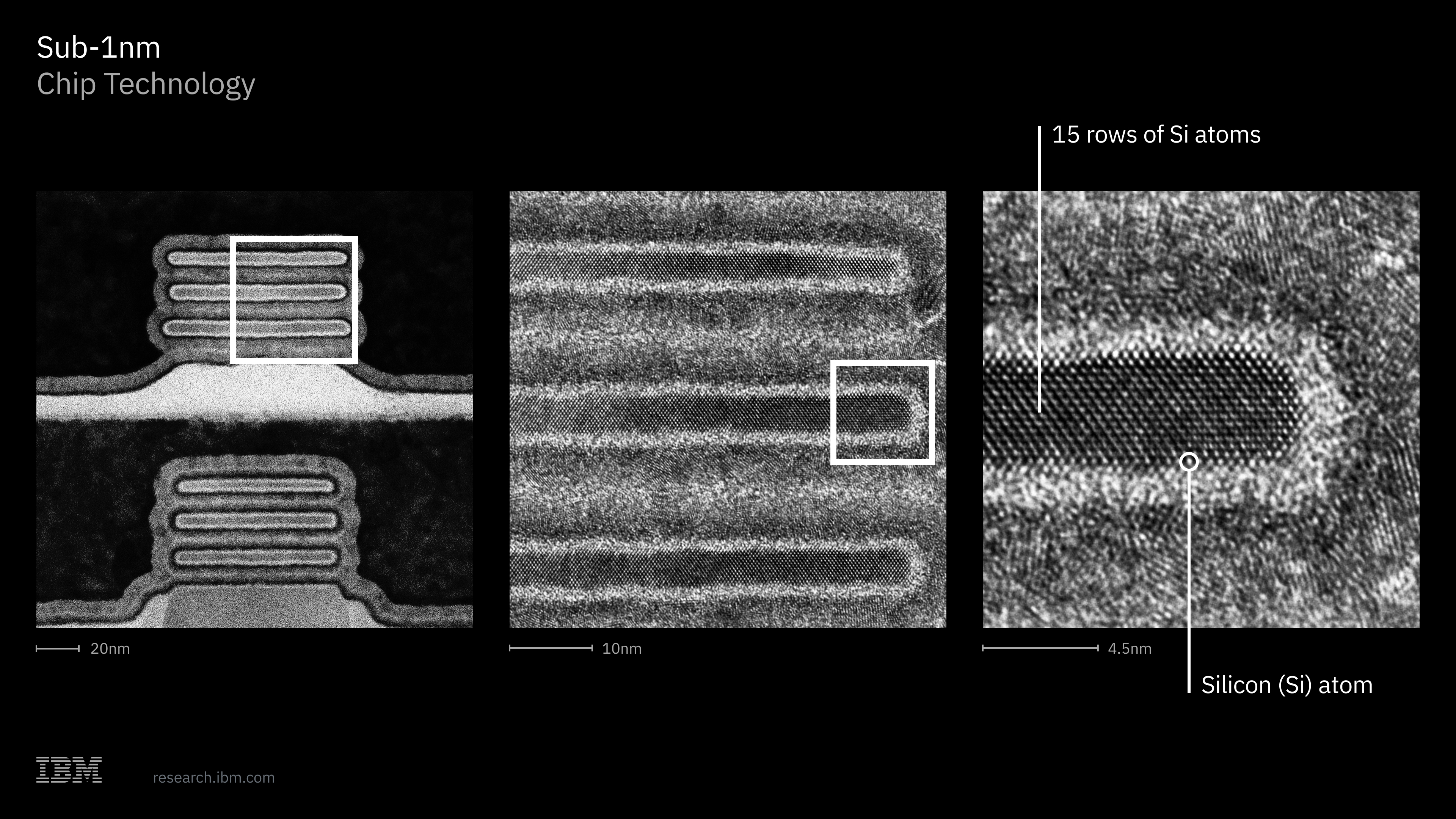
As it can be seen from the photos, horizontally the features are much bigger than 5 nm.
For silicon, the gate length of a FET has a lower limit somewhere between 10 nm and 15 nm.
The current CMOS manufacturing processes have not reached the limit yet. For making smaller transistors, a transition to other semiconductor materials will be necessary.
The vertical thicknesses of various layers may be of only a few nanometers or even of a fraction of a nanometer, but that does not matter directly for the circuit density.
The supposed node size refers to horizontal dimensions, not to vertical dimensions.
Vertical dimensions of around 1 nanometer or less could be achieved already many decades ago, because they depend on growth speed and on time, not on lithography, like the horizontal dimensions.
The industry should have stopped decades ago to talk about the "size" but they should have characterized a CMOS process by its density, e.g. in logic gates per square mm.
However, an actual concrete number would be disliked by marketing, because they could no longer claim that their "1 nm" process is better than the "2 nm" process of another vendor, if their density is not really better.
gabrielhidasy a day ago
Just get better marketers to say your 2nm process has more gates per sqmm than your competition 1nm process.
kailden a day ago
meindnoch 5 hours ago
>The vertical thicknesses of various layers may be of only a few nanometers or even of a fraction of a nanometer
We should flip the transistors sideways then!
scythe a day ago
The scale bar on the far right "photo" (micrograph?) doesn't make sense. It is only slightly less than half the scale bar on the middle photo (10 nm), but the image is clearly scaled up by much more than 2x. Individual silicon atoms are circled in the right photo, but the covalent radius of silicon is about 0.11 nm, so they should be much smaller if the scale bar is accurate.
wongarsu 8 hours ago
sylware 4 hours ago
Marketing scams has been the norm for the silicon industry for a big decade.
How would you fix that? This is a global scam. Big Markets regulating them: that would have to be the USA and EU.
u1hcw9nx a day ago
Unlike marketing terms, "nm density" is actually useful measure.
It describes density measure where you can compare it to planar transistors from the 28-nanometer (28 nm) node around 2010 to 2011 and before. A "0.7 nm" node has equivalent transistor density as if we could have shrunk standard flat transistor node down to 0.7 nanometers.
jayd16 21 hours ago
Why not use something absolute, like nand-gates per volume?
u1hcw9nx 19 hours ago
mikepurvis 21 hours ago
YetAnotherNick 8 hours ago
Why is density any bit important? All I care about is the price per transistor, and the power usage(mostly gate charge and leakage current?).
myrmidon 6 hours ago
jhide 5 hours ago
sbergot 3 hours ago
Smalltalker-80 20 hours ago
Yeah, the actual sizes are right there in the pictures, and never < 1 nm.
measurablefunc a day ago
Density is mass per volume so how are you comparing it to a planar transistor? Your units don't even match.
bandrami 10 hours ago
gruez a day ago
john_strinlai 21 hours ago
amirhirsch 21 hours ago
bronson a day ago
Legend2440 a day ago
It's been decades since published node sizes had any connection to actual feature size. Sadly this is just how it works in the semiconductor industry now.
amelius 21 hours ago
Who started it?
lizknope 19 hours ago
roelmore 20 hours ago
pseudosavant a day ago
My read on it was that they are trying to imply a transistor density (in a 2D plane sense) that is comparable to a 1nm process? But they achieve that through stacking (3D, not 2D) since the features aren't actually anywhere near 1nm?
makeitdouble a day ago
If they're adding a dimension, the marketing should reflect that.
I know they won't go for an anything that makes as much sense as 5nm3, so I vote for "1nm hyper space"
ncruces 8 hours ago
y1n0 a day ago
shash 15 hours ago
Correction: it’s not stacking. They do things like FinFET (turning the gates in the third dimension) and gate-all-around which increases the density of transistors per unit area. But they don’t have layers of transistors. At least in the logic and analog processes.
ktm5j 19 hours ago
What industry doesn't have a few too many marketers? Take everything with a grain of salt.
roflmaostc a day ago
yeah, where on the pictures is the 0.7nm feature? The linespacing is around 5nm. Is it the white line which is 0.7nm?
TallGuyShort a day ago
I really can't see where the 0.7nm is coming from. The white line looks like it's just an edge of a feature that is "15 rows of silicon atoms", which by some quick arithmetic on Wolfram Alpha has to be AT LEAST ~1.6nm, and the way the rows of atoms appear to be packed in that image and by the provided scale, it seems to be significantly more. Using the white line as a meaningful measurement seems to me to be more misleading than any other interpretation here.
wmf a day ago
sankalpmukim 10 hours ago
I believe it could be a stepping stone to significantly higher density in the future.
api a day ago
Better metrics are transistors/mm^2, performance/watt, and raw performance, since at this point "nm" is fluff and easily game-able.
Different companies measure it differently too. This was a while ago, but I remember reading that Intel 10nm was more or less close to TSMC 7nm. I'm sure this is still true to varying degrees.
shash 15 hours ago
Comparing nodes across foundries is a kind of a coin toss. At least, from the name. You actually need to go into the specifics of the pdk and process to understand what features there are. Can’t rely on the name for anything.
somesortofthing 19 hours ago
only a matter of time before some marketer figures out they can get promoted by branding a generation of chips 0nm
cyanydeez a day ago
On the otherhand, no investor really cares what it's called, they just need to know it's next gen.
formerly_proven a day ago
> Continuing the well established trend of making bold claims about physical dimensions that have nothing to do with any of the structures in the chip, and the name scales better than the tech.
We care about PPA (power, performance, area) and not how large or not-large features actually are. Comparing gate lengths between a 1980s planar transistor and a 2010s 3D FinFET or GAA transistor is obviously nonsense, the relatively aligned node names of the industry actually do make sense as a shortcut here.
colechristensen a day ago
You have to admit it's getting progressively sillier though.
Loic an hour ago
Looking at this picture: https://filecache.mediaroom.com/mr5mr_ibmnewsroom/201436/IBM...
I am just astonished at the quality of the structure. Not only that, but the quality of the "cut" to then be able to take this picture. I was closely involved in EM imaging more than 30 years ago, this is just wonderful to see such pictures now.
jadar a day ago
Just to be clear, this doesn't mean that anything on the die actually measures 0.7nm — it means that it's roughly double the density as the previous node generation. At some point the industry decided to keep talking about "nanometers" even though the actual transistor sizes have been decoupled from the node name for years.
zmgsabst 14 hours ago
Generations.
Gen Alpha were born since the naming became detached from actual physical size. And parts of Gen Z (before) and Gen Beta (after).
port11 12 hours ago
Naming generations is a futile, arbitrary process, whereas the measurement unit for engineering processes should be precise and well defined?
wongarsu 8 hours ago
zmgsabst 12 hours ago
IanCutress 18 hours ago
For what it's worth, here's my 7000+ word deep dive into the technology.
https://morethanmoore.substack.com/p/ibms-announces-07nm-pro...
zparky 14 hours ago
Hi Dr. Cutress! I loved reading your deep dives on Anand, they're what got me interested in semiconductors. Hope you're well <3
asah 5 hours ago
weird q: the photo shows a wafer with partial chips rendered on the edges?
lizknope 19 hours ago
Remember that IBM paid Global Foundries $1.5 billion to take their fabs and design services group.
GF did not pay IBM. IBM paid GF to take the fabs away.
https://www.reuters.com/article/technology/ibm-to-pay-global...
d3m0t3p 19 hours ago
It was 15 years ago. Whole management got replaced, they are quite ambitious. Let's see if how this works out now.
trynumber9 15 hours ago
The plan doesn't involve running fabs again. Too expensive. IBM licenses their manufacturing technology (so far to Rapidus in Japan).
alexey-salmin a day ago
The most surprising part for me is that IBM still somehow owns silicon labs, I was sure it's effectively a consulting company by now
dekhn a day ago
Most of their fabs were divested to GlobalFoundries, but they still have pretty significant fab capability and capacity- I suspect at least partly to have a us-based chip-making for military ("Trusted Foundry").
turtletontine a day ago
The labs might not be that different from consulting, the NYT reporting on this notes they run R&D labs so they can license the tech they develop to people who actually make chips.
Barrin92 a day ago
IBM has been the company with the most patent registrations in the US for I think 29 of the last 30 years. They're one of the largest industrial research organizations in the world. They're doing more hard science research than almost anyone else.
smokefoot 21 hours ago
Which is so weird, right? Like what is IBM now and how does a research lab make sense with the rest of their business?
The money-making parts of IBM are: legacy software and hardware (declining), consulting (low margin, low leverage), enterprise software (mostly redhat, not really growing). It's hard to explain how IBM research is accretive to any of that.
rbanffy 21 hours ago
orbifold 15 hours ago
macintux 21 hours ago
PhilipRoman 6 hours ago
AlexCoventry 21 hours ago
It's just a shame that none of it seems to pan out, and in the areas where I know what they're talking about, it all sounds like cynical nonsense to me.
girvo 19 hours ago
I really wish I had followed through when I was ask by some of the guys at IBM Research to apply when we had worked together on a partner project. Though I didn’t have a degree which I seem to remember was a sticking point, this is in the mid 2010s
throw0101d a day ago
One of the images has "15 rows of Si atoms".
Is there a limit to how small things can go? A single atom?
Is there a physical/molecular limit to Moore's Law?
vitally3643 a day ago
Yes, and we're already there. We've been there for quite a while, in fact.
Once you make the gate of a transistor small/thin enough, quantum effects take over. Electrons will randomly teleport into and through the gate causing the transistor to conduct when it shouldn't. I don't have numbers to hand, but it's on the order of a few atoms wide. There's really nothing that can be done about it either, as far as we know. Electrons just aren't physical objects at this scale, you can't simply exclude them from any given volume of space. The electron wave function will simply just appear wherever it wants (within the electron probability cloud). The only way to stop it is to make your insulating junction thicker than the probability cloud.
BitwiseFool a day ago
>"The electron wave function will simply just appear wherever it wants (within the electron probability cloud)."
I don't know which is more ridiculous, the fact that reality works like this, or, that a species of apes was able to figure this out.
anvuong 21 hours ago
vitally3643 20 hours ago
rvba 9 hours ago
HerbManic 15 hours ago
This is why I suspect we will be neat the upper limits of this around the late 2030's. We are just running too close to the fundamental limits. And so far there isn't anything really radical even on the horizon as a solution for this.
rswail 5 hours ago
marcosdumay 21 hours ago
> you can't simply exclude them from any given volume of space...
... inside a silicon crystal.
You can keep the electrons into as small a volume as you want, but you need something there forcing them, and doped silicon will only force them so much.
In fact, those transistors are smaller than what a silicon crystal can do, and the electrons are only held there because they are made of more materials than only silicon.
wmf a day ago
throw0101d a day ago
> https://en.wikipedia.org/wiki/There%27s_Plenty_of_Room_at_th...
Yes, single-atom manipulation has already been demonstrated:
* https://en.wikipedia.org/wiki/IBM_(atoms)
Can you make transistors using that technique? Can you smaller?
dgfl 20 hours ago
colechristensen a day ago
I mean, you can't get smaller than an atom, there is some amount of plausibility of using individual atoms as at least the occasional computing element.
Beyond that, engineering a quark-gluon plasma as a processor? I'd watch that Star Trek episode. (we might fantasize about stuff like that but we're roughly monkeys smashing rocks together in a cave vs. building an iPhone sort of gap away from that kind of thing unless somebody has a really good idea)
mrandish 18 hours ago
> you can't get smaller than ...
I always thought the true limit was the Planck length against which an atom is giant. There's a whole zoo of sub-atomic particles but I don't think we know how (or if) we can apply those for practical computing.
Gravityloss 18 hours ago
A physicist can fill in but there might be some stuff made out of subatomic particles for example.
vitally3643 a day ago
You could, in principle, use photons and/or electrons. We got pretty damn close in the vacuum tube era, and photonic computing has been a popular research topic for a while.
You also have quantum computing, which I think can/does use subatomic particles? Not sure about that one
dgfl 20 hours ago
HarHarVeryFunny a day ago
superjan a day ago
dataflow a day ago
mrguyorama 21 hours ago
masswerk 3 hours ago
How do these 3D architectures scale regarding yield? (The naïve expectation would be that adding vertical layers should have exponential impact on yield.) Is this commercially viable, near term?
giwook a day ago
How does IBM commercialize this? Do they license this out to fabs?
topspin a day ago
> Do they license this out to fabs?
Broadly speaking yes, this is the business model. IBM has been at this for many years with technology transfers, licensing agreements, support and other arrangements. Rapidus, Samsung, GlobalFoundries, ST, SMIC, AMD, etc. have all used IBM R&D work at various times for various nodes and products.
The cutting edge of semiconductors is a writhing mass of copulating tapeworms, and IBM lives deep inside that ball. For IBM, what this means is that when you buy one of the ASML machines to make products with this process, you'll pay IBM for the knowledge and support to actually get it working, or give them a cut, or something else, TBD, as circumstances warrant.
dboreham 16 hours ago
Ah, thanks for that explanation. I was wondering how IBM could fund cutting edge research in semiconductors when they haven't been a semiconductor manufacturer for many years.
jcgrillo 17 hours ago
> a writhing mass of copulating tapeworms
What a metaphor! I will file that one away for some glorious future opportunity.
topspin 17 hours ago
wmf a day ago
They licensed 2 nm to Rapidus so yes.
drob518 a day ago
I’m sure they will license it. It’s better for them if everyone in the industry can innovate on everything around it. All the process tech companies will make it more cost effective, for instance, which helps IBM as well.
Danox 19 hours ago
A sad ending for one of great American companies...
evanjrowley a day ago
boost sales for their systems division, POWER CPUs, mainframes, maybe Quantum stuff
TallGuyShort a day ago
I always feel like I'm not quite getting quantum stuff no matter how much I read and learn: what does this advancement have to do with quantum computers?
amirhirsch 21 hours ago
WaxProlix a day ago
Sit on a patent and try to scrape earnings from others, maybe? That is, license or litigate.
victor106 a day ago
Keep hearing that IBM makes these incredible chips but don’t see anyone using IBM chips. What do they do with them?
xxpor a day ago
Approximately everyone (at least in the F500) outside of Big Tech uses them. For example, Costco's entire inventory management system runs on IBM i (so, POWER). You can see the classic terminal look around the store. Banks run a TON of z and i. You'll never see them because they're essentially always in data centers, but I guarantee you interact with them even if it's very non-obvious because there's 50 microservices between the UI and the actual system of record.
HerbManic 15 hours ago
And some of those i and z systems have some obscene engineering in them. I cannot find it now but i remember seeing a cross section of their 40 layer PCB simply so they could get more memory/IO performance to the CPU. POWER may have dropped out of the consumer space but it still has a vital place in servers.
reppap 19 hours ago
Ericsson used a lot of power chips in their telecom hardware 10 years ago at least, haven't worked with their stuff since then so I haven't kept up.
ternaryoperator 20 hours ago
Their line of POWER chips are used in their mainframes
lizknope 19 hours ago
No, their mainframes use the zArch which goes back to the System/360 from 1964.
https://en.wikipedia.org/wiki/Z/Architecture
IBM sells huge servers with POWER architecture CPUs but they are not what people are referring to when they talk about IBM mainframes.
kcb 21 hours ago
The product here is the research and licensing the tech.
jjk7 a day ago
usgov
monirmamoun a day ago
Two big problems 1) NOBODY knows what IBM's definition of "sub 1nm" means 2) IBM bullshits so much more than anyone including Intel (remember the "teleportation" ads years ago) that nobody is going to waste time researching what they mean in reality
wasabi991011 21 hours ago
> remember the "teleportation" ads years ago
Never heard of this, care to elaborate?
duckmysick 20 hours ago
I think the OP references Intel ads with Jim Parsons from like a decade ago.
https://www.youtube.com/watch?v=PQWpYQm60P4
There were more of them, including some with other celebrities.
cryptoegorophy 20 hours ago
Maybe it is done to pump their stock with low effort? It seems that way for many companies.
wmf a day ago
I know what it means. Something isn't automatically bullshit because it's outside your field of expertise.
pjmlp 11 hours ago
People love to hate on IBM, ask why it is relevant today, while several of their beloved FOSS projects are in some way, form or fashion, made possible with IBM's money.
Oras 5 hours ago
cr3ative a day ago
“I’m able to parse a marketing term” isn’t a great claim here. Pointing out it’s an unclear term largely abused is valid.
wmf 21 hours ago
petcat a day ago
> IBM and its partners conduct this work at a leading semiconductor research facility in Albany, New York, which will soon be home to a High Numerical Aperture Extreme Ultraviolet (High NA EUV) lithography tool, essential for the future of logic scaling. Developed by ASML, this technology enables ultra‑precise circuit printing, supporting the creation of smaller, more powerful chips.
I'm guessing that this is the technology that is developed by Cymer (ASML subsidiary) in California, correct? Is there competing technology? I know xLight is trying to make some inroads on their own version of this EUV tech. I have not heard about any progress though.
scrlk a day ago
Cymer builds the EUV light source, but the biggest enabler for High NA EUV is using anamorphic optics (ie asymmetric horizontal and vertical magnification) from Zeiss: https://www.asml.com/en/news/stories/2024/5-things-high-na-e...
porridgeraisin a day ago
Correct
Alien1Being 15 hours ago
More marketing lies from IBM. Sad to see the decline and corruption of a once OK company.
Selling a 5 nm vertically stacked chip as equivalent to 0.7 nm
Shades of Watson and other IBM lies.
elisbce a day ago
Why doesn't the industry use something like transistor density per cubic cm? This would extend to 3d cases and impossible to fake
zamadatix a day ago
The industry does use a collection of more practical measurements, like transistor density. Marketing pieces for the news tend to use this kind of jargon precisely because it can be fudged & it sounds like it means something else than it really does to the average person. It's also simple enough to avoid needing to really explain what kinds of numbers are impressive etc, everyone just knows less than 1 nm is tiny and they've heard X nm for decades to compare to at this point.
spzeno 11 hours ago
Is the 3D transistor proposed by IBM on the same track as Tao's Law proposed by Huawei?
markhahn a day ago
has anyone found a paper with details?
also, I was expecting to see cfets mentioned.
kosolam 8 hours ago
They dont give the exact size hmm
cubefox 19 hours ago
Relevant quote:
> IBM sees a path to production in as early as the next 5 years.
5 years is a long time for a product roadmap, so there are probably some significant unsolved problems remaining, and the timeline depends on whether IBM can solve these problems.
applfanboysbgon a day ago
For anyone who needs it, a friendly reminder that CPU nm marketing is a complete fabrication and the physical size of transistors has zero relation to the marketing claims. These are not, in fact, physically sub 1 nm, despite the bombastic claims.
lp4v4n a day ago
>These are not, in fact, physically sub 1 nm, despite the bombastic claims.
Why? What's their real size?
Not doubting you, just trying to understand and also trying to assess how exaggerated the marketing is.
CAP_NET_ADMIN a day ago
At some point in the transistor scaling, the electrons started leaking across the gate, we've switched from 2D design to 3D structures to prevent that, so the actual physical gate pitch for like the TSMC 3nm is around 45 nm in distance.
Currently thrown around numbers mean the "equivalent performance/density" or something like that.
applfanboysbgon a day ago
They don't describe the exact physical size (that would rather defeat the point of the marketing), but you can see the photographs at the bottom have a scale measured in tens of nm.
wmf a day ago
The marketing nm better represent the density and performance of the transistors than the actual feature size, especially in this case.
micw a day ago
So the title should be corrected. The did not debut sub nm chips at all.
antisthenes a day ago
That ship sailed long ago. I think it was around 32nm-22nm node when the marketing term started diverging from the physical feature size.
micw 19 hours ago
sidcool 14 hours ago
How come we don't hear anything about Watson?
EagnaIonat 11 hours ago
Well Watson went from a product, to product line branding. Then changed to Watsonx.
Doing a search on that there are loads of news articles.
georgeburdell 21 hours ago
IBM debuts a PDK and some test structures, as they have no production fabs
rbanffy 21 hours ago
They have small scale fabrication capabilities or they wouldn’t be able to validate the technology enough to sell it.
georgeburdell 17 hours ago
Tell me where I said they didn’t have fabs
bozhark 18 hours ago
Sub-Atomic level chips soon, then?
glaslong 4 hours ago
Yes, shortly followed by negative space chips
rvba 9 hours ago
Isnt that quantum computing?
perching_aix a day ago
I wonder at what point does it become deceptive in the legally biting way to market process nodes like this. One can wax and wane a bunch about industry terminology status quo, but this is mental.
kitd 20 hours ago
It'll be a brave man who takes on the IBM legal department over terminology in widespread use.
stackedinserter a day ago
Since a transistor can't be smaller than a single atom, maybe it's time to start optimizing our software again.
ginko a day ago
IBM regularly announces silicon breakthroughs like this but I'm not aware of those ever becoming products. Is IBM mainly in the business of licensing their technology to big silicon manufacturers with stuff like this? Is it just marketing for their consulting business?
vessenes a day ago
My understanding is they are largely an IP business. That said this release mentioned an ASML machine on prem, so?
ijidak a day ago
IBM's contributions to computing hardware and software are incalculable.
So many breakthroughs in hard drives, chips, transistor density, and other aspects of computing have come out of their labs.
Great to see them continuing to innovate.
But, yeah, usually they partner and license. Over the years, they've spun off more and more of their hardware businesses.
petra a day ago
It's great that they found a working business model for a pure r&d lab, and with such awesome results.
I wonder why isn't this more common.
bruckie a day ago
Don't forget copper interconnects for ICs. https://www.chiphistory.org/ibm-s-development-of-copper-inte...
AnimalMuppet a day ago
I believe that IBM makes the chips for their Z Series mainframes. I mean, that's low volume production, but they need small feature size.
nradov a day ago
IBM Z series mainframe Telum CPUs are designed by IBM but manufactured by Samsung. IBM no longer owns any fabs. I assume they have some kind of technology licensing deal.
ac29 a day ago
greenavocado 18 hours ago
Not bad, now you just have to fold it 86 times to reach one Planck length. The only issue you'd run into is it would have to be 77 quadrillion kilometers thick
mxuribe a day ago
A little bit of a nitpick, but wouldn't that be a picometer instead of angstrom node? Like, isn't a "pico-" the next magnitude smaller than "nano-", or am i wrong?
Otherwise, that chip tech sounds really awesome - at least for the future!
saulpw a day ago
There are 3 orders of magnitude between nano (^-9) and pico (^-12). An Angstrom is ^-10m.
1313ed01 a day ago
Useless fact I just learned from Wikipedia: Ångström/Angstrom (in Sweden of course we still use the original spelling) has its own UNICODE symbol, Angstrom sign: Å (U+212B) not to confuse with the Swedish letter Å (U+00C5). Looks slightly different in my browser.
nielsbot a day ago
mxuribe a day ago
Aaahhh, ok, thanks!
applfanboysbgon a day ago
Romario77 a day ago
Because 1 angstrom equals 10⁻¹⁰ meters and 1 picometer equals 10⁻¹² meters, the relationship is:
1 Å = 100 pm. 1 pm = 0.01 Å.
TallGuyShort a day ago
1 picometer = 0.001 nanometers, 0.01 angstrom
1 angstrom = 0.1 nanometers, 100 picometers
1 nanometer = 10 angstroms, 1000 picometers